N
TruthVerse News

How do I program a CPLD Xilinx?

Author

Avery Gonzales

Updated on March 14, 2026

How do I program a CPLD Xilinx?

To program the programming file into the CPLD connect the JTAG pins of the CPLD to the programming adapter, power the CPLD and adapter (5V for XC9500 family and 3.3V for XC9500XL family). Expand the Generate Programming File and select Configure Device (iMPACT). Use the default options. Enjoy.

People also ask, how do you program a CPLD?

Open the iMPACT programming tool from the ISE Design Suite project panel under Configure target device->iMPACT. Choose the option to create a boundary scan file, and set the type to XSVF. Give the XSVF output a file name and then add a compiled CPLD image (ex1. jed) when prompted to add a device.

Beside above, what is a macrocell in CPLD? Macrocells are the main building blocks of a CPLD, which contain complex logic operations and logic for implementing disjunctive normal form expressions. Macrocells can also be defined as functional blocks responsible for performing sequential or combinatorial logic.

Beside above, how do I program Xilinx?

Programming the FPGA

  1. Select Xilinx Tools > Program FPGA.
  2. In the Bitstream and BMM File fields, specify the bitstream (. bit) and Block RAM Memory Map (.
  3. SDK automatically detects the processors in the system and shows them in a table at the bottom of the window. Under Software Configuration, select the executable (.
  4. Click Program.

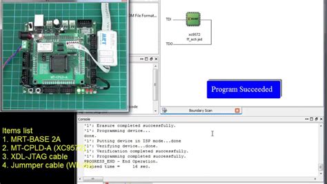
What is a .JED file?

A JED file is a Xilinx JEDEC hardware configuration file. It is used for programming complex programmable logic devices (CPLDs), such as computer processors. ISC files, which are used for programming FPGA hardware devices. Important: JEDEC is an acronym for "Joint Electron Device Engineering Council."

How are programmable logic devices programmed?

A programmable logic device (PLD) is an electronic component used to build reconfigurable digital circuits. Unlike integrated circuits (IC) which consist of logic gates and have a fixed function, a PLD has an undefined function at the time of manufacture.

What is the difference between FPGA and CPLD?

The primary differences between CPLD and FPGA are architectural. A CPLD has a restrictive structure which results in less flexibility. The FPGA architecture is dominated by interconnects, which makes them not only far more flexible but also far more complex to design.

What is CPLD used for?

CPLD is used for loading the configuration data of a field programmable gate array from non-volatile memory. CPLDs are frequently used many applications like in cost sensitive, battery operated portable devices due to its low size and usage of low power.

What are programmable chips?

A programmable chip is an electronic component that contains a series of instructions that are executed each time the chip functions. These chips are the cornerstone of modern electronics; they are present in nearly every electronic device.

What is CPLD firmware?

A complex programmable logic device (CPLD) is a programmable logic device with complexity between that of PALs and FPGAs, and architectural features of both. The main building block of the CPLD is a macrocell, which contains logic implementing disjunctive normal form expressions and more specialized logic operations.

How do you program FPGA?

How to Program Your First FPGA Device
  1. Materials. Hardware. Software.
  2. Step 1: Create an Intel® Quartus® Software Project.
  3. Step 2: Create an HDL File. Hardware Description Language (HDL) Change the Blink Rate.
  4. Step 3: Create a Verilog Module.
  5. Step 4: Choose Pin Assignments.
  6. Step 5: Create an SDC File.
  7. Step 6: Compile the Verilog Code.
  8. Step 7: Program the FPGA.

How do I program a FPGA JTAG?

To program via JTAG:
  1. Make sure the programming jumper is in the JTAG position.
  2. Click program device, select the device, and select the correct bit file.
  3. Click program.

How do I download FPGA programs?

  1. Step 1: Download and Install ISE WebPACK Design Software. Xilinx provides a free IDE software named ISE WebPACK for beginners.
  2. Step 2: Setup Xilinx Platform Cable.
  3. Step 3: Create Your First FPGA Project.
  4. Step 4: Program Your FPGA.
  5. Step 5: Download the Program to SPI Flash.

How do I burn Xilinx program to FPGA?

Step by Step procedure to run a program on FPGA board
  1. STEP1: Open Xilinx ISE and create a new project.
  2. Project summery window occurs.
  3. Step 3: Click on Project > New Source.
  4. Step 4: Select Source type is Verilog Module and enter the file name (ANDing_code).
  5. Step 5: Define Module Window.
  6. Step 6: Summery Window.
  7. Step 7: The Project Navigator window looks like below window.

What are different types of FPGA programming modes?

There are two basic modes of programming: Master mode, when FPGA reads configuration data from an external source, such as an external Flash memory chip. Slave mode, when FPGA is configured by an external master device, such as a processor.

What is Xilinx iMPACT?

iMPACT, a tool featuring batch and GUI operations, allows you to perform the following functions: Device Configuration and File Generation. File Generation enables you to create the following types of programming files; System ACE CF, PROM, SVF, STAPL, and XSVF files.

What is configuration memory?

2) Config memory holds the information on how your part was programmed and therefore implements your design. 3) There is a table in UG470. But again, you are not concerned about the actual number of configuration cells in the part (other than for your configuration memory device..SPI, BPI or so).

What is Xilinx SDK?

The Xilinx® Software Development Kit (SDK) provides an environment for creating software platforms and applications targeted for Xilinx embedded processors. SDK works with hardware designs created with Vivado®. SDK is based on the Eclipse open source standard.

What is bit file in FPGA?

An FPGA bitstream is a file that contains the programming information for an FPGA. A Xilinx FPGA device must be programmed using a specific bitstream in order for it to behave as an embedded hardware platform. This bitstream is typically provided by the hardware designer who creates the embedded platform.

What is mean by FPGA?

Field Programmable Gate Arrays

Why have PLDs taken over so much of the market?

25. Why have PLDs taken over so much of the market? One PLD does the work of many ICs. The PLDs are cheaper.

What is FPGA architecture?

A basic FPGA architecture (Figure 1) consists of thousands of fundamental elements called configurable logic blocks (CLBs) surrounded by a system of programmable interconnects, called a fabric, that routes signals between CLBs. Input/output (I/O) blocks interface between the FPGA and external devices.

What are the outputs of AND gate in PLD is said to be?

Explanation: Outputs of the AND gate in PLD is known as output lines. Explanation: Programmable Logic Array is a type of fixed architecture logic devices with programmable AND gates followed by programmable OR gates. It is a kind of PLD. Explanation: Since, PLA is a combination of programmable AND and OR gates.

What is another name for digital circuitry called sequential logic?

12. What is another name for digital circuitry called sequential logic? C.

Exercise :: Programmable Logic Device - General Questions.

A.PAL
D.SRAM

What are the essential capabilities that we need in an FPGA?

What are the essential capabilities that we need to get from an FPGA? First, it needs to provide ample amounts of logic. The more the better, as the value tends to rise faster than cause as FPGAs get large. Smaller FPGA process geometries usually translate in the higher logic density.

What is Gal in digital electronics?

The Generic Array Logic (also known as GAL and sometimes as gate array logic) device was an innovation of the PAL and was invented by Lattice Semiconductor.

What is memory decoding in digital electronics?

Explanation: The Memory IC used in a digital system is selected or enabled only for the range of addresses assigned to it and this process is called memory decoding. It decodes the memory to be selected for a specific address.

What is CPLD in VLSI?

A complex programmable logic device (CPLD) is a semiconductor device containing programmable blocks called macro cell, which contains logic implementing disjunctive normal form expressions and more specialized logic operations. CPLD is used to load configuration data for an FPGA from non-volatile memory.